Low-Cost SPAD Sensing for Non-Line-Of-Sight Tracking, Material Classification and Depth Imaging
SIGGRAPH 2021

We propose the use of cheap, small off-the-shelf distance sensors (far left) for a variety of computational imaging and vision tasks, and demonstrate and evaluate their capabilities in emerging sensing applications like (from left to right) material classification, non-line-of-sight tracking, and depth imaging.
Time-correlated imaging is an emerging sensing modality that has been shown to enable promising application scenarios, including lidar ranging, fluorescence lifetime imaging, and even non-line-of-sight sensing. A leading technology for obtaining time-correlated light measurements are single-photon avalanche diodes (SPADs), which are extremely sensitive and capable of temporal resolution on the order of tens of picoseconds. However, the rare and expensive optical setups used by researchers have so far prohibited these novel sensing techniques from entering the mass market. Fortunately, SPADs also exist in a radically cheaper and more power-efficient version that has been widely deployed as proximity sensors in mobile devices for almost a decade. These commodity SPAD sensors can be obtained at a mere few cents per detector pixel. However, their inferior data quality and severe technical drawbacks compared to their high-end counterparts necessitate the use of additional optics and suitable processing algorithms. In this paper, we adopt an existing evaluation platform for commodity SPAD sensors, and modify it to unlock time-of-flight (ToF) histogramming and hence computational imaging. Based on this platform, we develop and demonstrate a family of hardware/software systems that, for the first time, implement applications that had so far been limited to significantly more advanced, higher-priced setups: direct ToF depth imaging, non-line-of-sight object tracking, and material classification.
Low-Cost SPAD Sensing for Non-Line-Of-Sight Tracking, Material Classification and Depth Imaging
Clara Callenberg, Zheng Shi, Felix Heide, Matthias B. Hullin
SIGGRAPH 2021
Video Summary
Low-Cost SPAD System
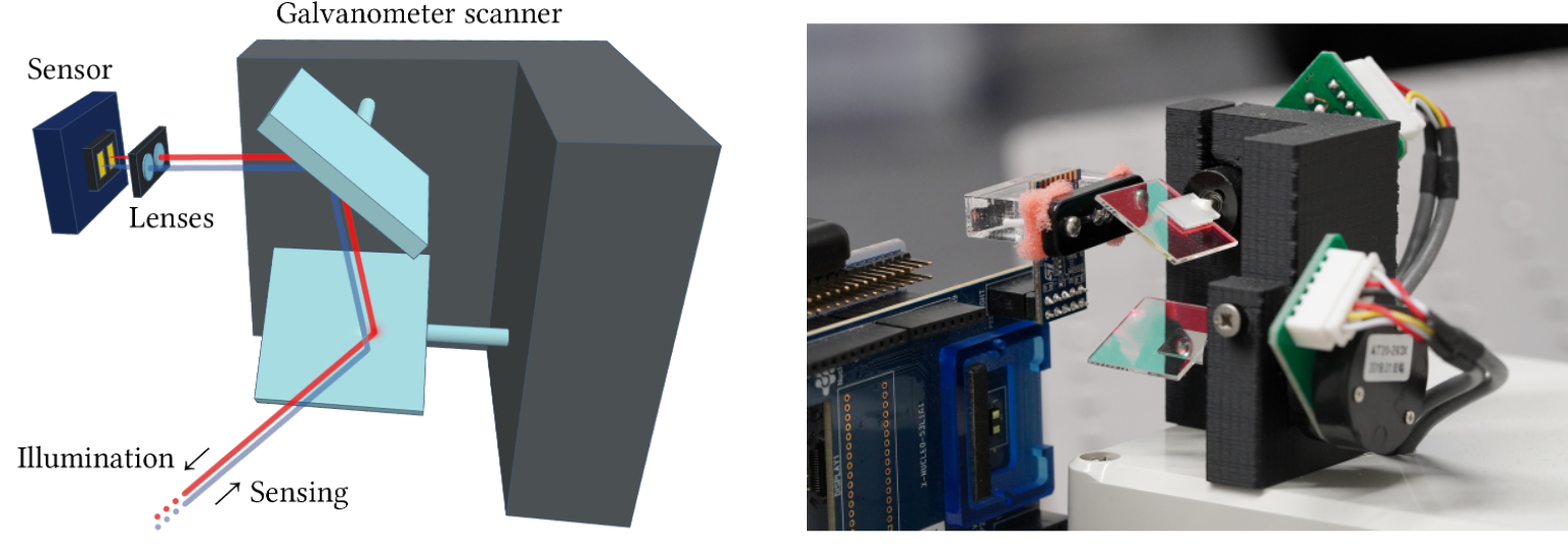
The centerpiece of our system is the VL53L1X time-of-flight sensor module by STMicroelectronics. The 12-pin package, priced around USD 3 for large volumes, has a footprint of 15mm^2 and integrates a 940nm light source and a 16X16 SPAD array sensor with a field of view of 27 degrees imaged by a miniature lens. Ambient light influx is reduced by an appropriate filter. For some of the applications demonstrated in this paper, we use additional optical equipments including glasses and galvanometer scanners for increased flexibility of the system.
At a total system cost of USD 150 including all parts, our prototype system in the most expensive configuration is two to three orders of magnitude lower in cost than existing time-tagged research instrumentation.
Material Classification
We use the VL53L1X to classify different materials based on their temporal and spatial response to the illumination emitted by the device. When placing the sensor right onto the surface of a material, the infrared light from the VL53L1X light source penetrates the material, is scattered inside, and part of it is reflected back to the SPAD sensor. Depending on the structure of the material, the signal measured by the sensor can vary temporally and spatially. By training a neural network, characteristics of different materials can be learned and they can later be distinguished by holding the sensor to an object.
Tracking Objects “Around the Corner”
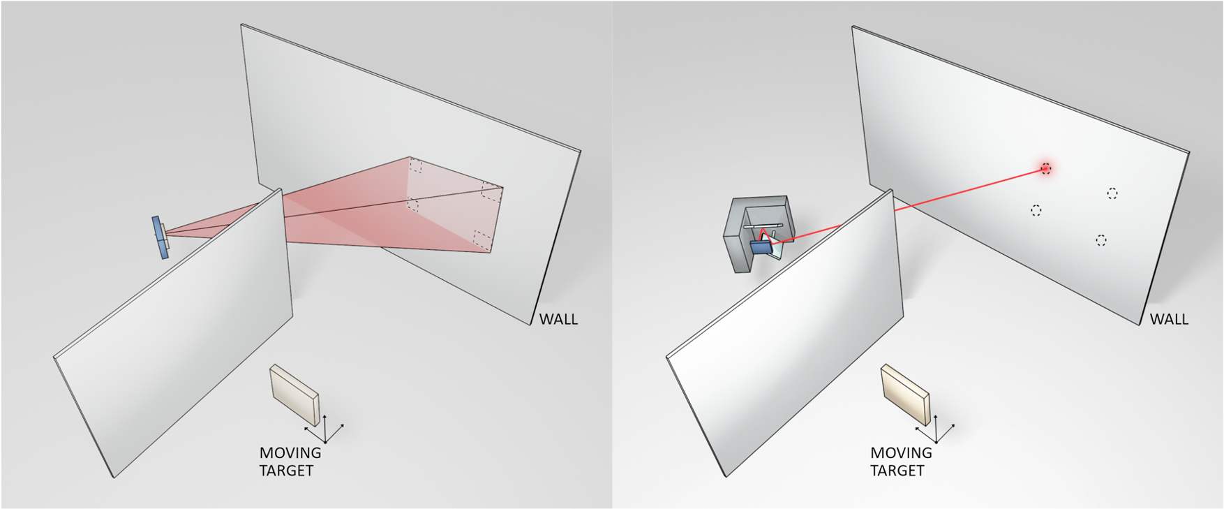
Observing objects hidden from the direct line of sight is a common application of time-resolved imagers. We show that the VL53L1X can be used to track an object “around the corner” by illuminating a wall facing the hidden area and recording the echoing light signal that is reflected from the target object. To this end, we train a neural network to recognize the target position from the SPAD data of four measurements on the wall.

Two variants of NLOS tracking setting.
Depth Imaging
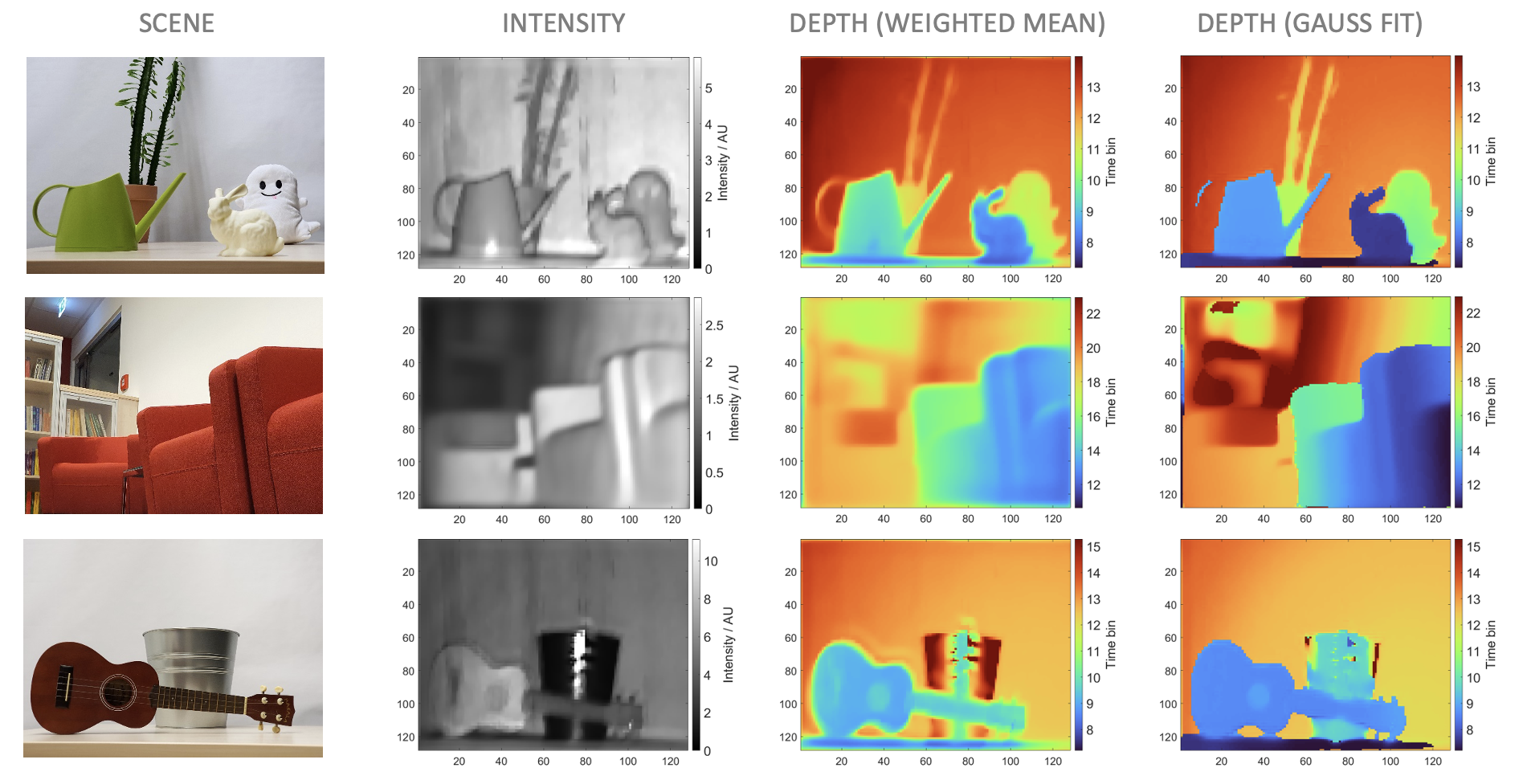
The VL53L1X can yield a spatially resolved transient image by scanning all possible 4×4 ROIs on the 16×16 pixel sensor, which yields a 13×13 pixel measurement. We use additional glasses and galvanometer scanners to avoid the substantial blur due to the overlapping ROIs and the poor optical quality of the imaging lens.

Depth maps are calculated in two different ways: (1) we calculate the given pixel’s depth as the weighted mean of the captured histogram. This way we achieve even smooth depth gradients and sub-bin accuracy in the depth estimation; and (2) we compute the depth by fitting Gaussian functions to the histogram of each pixel, which yields sharper and more reliable results at the cost of a longer runtime.

